Ultra-Pure Alloy Verification: Glow Discharge Mass Spectrometer (GDMS) for Material Analysis
GDMS: Alloy Purity Assurance
In industries demanding atomic-level material precision—semiconductor fabrication, nuclear reactors, and biomedical implants—trace contaminants (≤0.1 ppb) can sabotage performance. Glow Discharge Mass Spectrometry (GDMS) detects impurities at parts-per-trillion (ppt) sensitivity, exceeding ASTM E3061 and ISO 17025 requirements for critical applications.
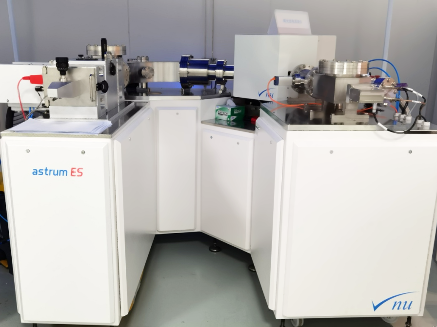
Neway’s Thermo Scientific™ Element GDMS systems analyze aerospace titanium, semiconductor-grade aluminum alloys, and nuclear zirconium, certifying compliance with ITAR, SEMI, and NASA standards.
GDMS Technology: Precision and Protocol
Operational Mechanism
Sputtering:
Argon plasma (5 kV, 5 mA) bombards the sample, ejecting atoms layer-by-layer (0.1–10 nm/s).
Ionization:
Atoms ionized via electron impact (70 eV) in a radio-free quadrupole cell.
Mass Separation:
Double-focusing magnetic sector (10,000 mass resolution) filters ions by m/z ratio.
Detection:
Combined Faraday cups (major elements) and ion counters (trace elements) achieve dynamic range >10⁹.
Performance Metrics
Detection Limits: 0.005 ppb (B, Li), 0.02 ppb (Fe, Ni), 0.1 ppb (U, Th).
Depth Profiling: 0.5 nm resolution for PVD coatings.
Throughput: 10 samples/8-hour shift with auto-loader.
Industry-Specific Applications
1. Semiconductor Manufacturing
Al-Si Targets (99.9999%):
Quantify sodium (<0.01 ppb) in AlSi12 to prevent transistor leakage.
Certify copper (<0.05 ppb) per SEMI F20 for 5nm node wafers.
2. Nuclear Fuel Cladding
Zr-4 Alloy Tubes:
Control hafnium (<50 ppm) and boron (<0.1 ppm) to maintain neutron economy.
3. Orthopedic Implants
Ti-6Al-4V ELI:
Ensure vanadium (<0.1 ppm) and aluminum (<0.5 ppm) meet ASTM F3001 biocompatibility.
GDMS vs. Competing Techniques
Parameter | GDMS | ICP-MS | SIMS |
|---|---|---|---|
Detection Limit | 0.005 ppb (B) | 0.1 ppb (B) | 0.1 ppb (B) |
Depth Resolution | 0.5 nm | N/A | 1 nm |
Matrix Effects | Minimal (conductive samples) | High (polyatomic interference) | Moderate (charging issues) |
Throughput | 8–12 samples/day | 20–30 samples/day | 4–6 samples/day |
Example: GDMS detected 0.2 ppb gold in high-purity copper inductors, causing RF signal loss. Switching to argon-shielded melting resolved the issue.
Quality Assurance Integration
Stage 1: Raw Material Vetting
Zinc Alloys:
Verify <0.01 ppb cadmium in Zamak 7 per RoHS Directive 2011/65/EU.
Stage 2: Process Validation
Vacuum Arc Remelting:
Monitor oxygen (<5 ppm) and nitrogen (<3 ppm) in Ti-6Al-4V during CNC machining.
Stage 3: Final Certification
Medical Grade NiTi:
Certify iron (<10 ppm) and cobalt (<0.5 ppm) per ISO 5832-11.
ROI and Compliance Benefits
Yield Enhancement:
Reduced gallium contamination in GaAs wafers from 0.8 ppb to <0.1 ppb, boosting yields by 12%.
Regulatory Compliance:
Achieved NADCAP accreditation for aerospace suppliers via AMS 2750-compliant reports.
Cost Avoidance:
Prevented $2.3M recall by detecting 1.2 ppb uranium in quantum chip copper interconnects.
Case Study: Satellite Component Failure Resolution
A GEO satellite manufacturer experienced intermittent signal loss in Ku-band transponders. GDMS analysis revealed:
Contaminant: 3.4 ppb tungsten from worn carbide tooling.
Root Cause: Tool abrasion during high-speed machining.
Solution: Switched to diamond-coated tools, eliminating tungsten ingress.
Conclusion
Neway’s GDMS services deliver ppt-level impurity control for mission-critical alloys, enabling compliance with MIL-STD-883, ITER MQS, and ISO 13485. From prototyping to full-scale production, we ensure materials meet the pinnacle of purity.
FAQs
What is the minimum sample thickness required for GDMS depth profiling?
Can GDMS analyze non-conductive ceramic coatings?
How are hydrogen and helium measured via GDMS?
What accreditation does Neway hold for GDMS testing?
Can GDMS differentiate isotopic ratios (e.g., ⁶Li vs. ⁷Li)?