Can Copper Anodizing Preserve Electrical Conductivity?
A copper surface treatment can preserve electrical function only when the required contact surfaces, film behavior, masking, fixture contact, and verification method are defined. A treatment film may change the contact interface even if the copper beneath it remains conductive. Therefore, a buyer should not approve “anodized copper” on appearance alone or assume that a process used on aluminum will preserve a copper contact. The electrical requirement must be checked on the finished part at the same interface used in the assembly.
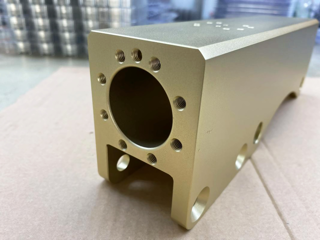
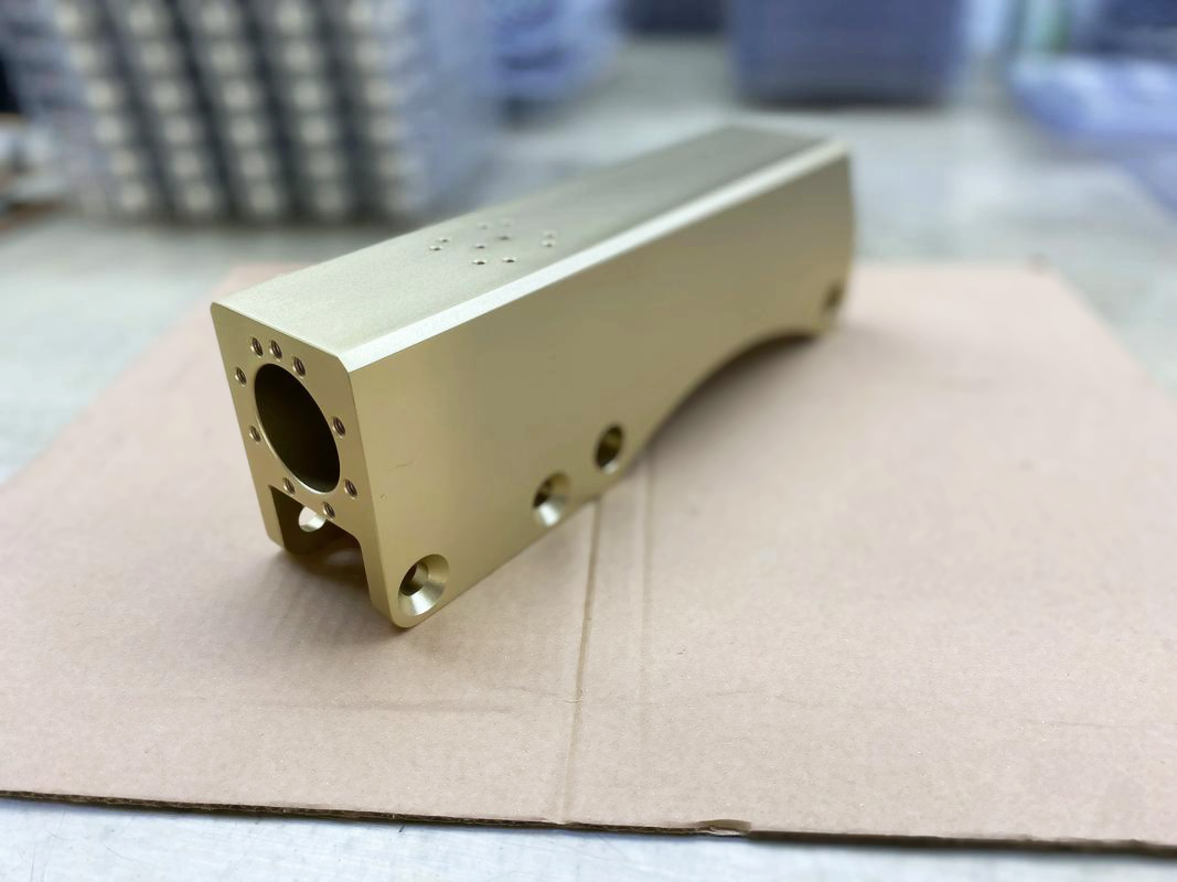
The first decision is whether the visible body and the electrical contact need the same surface. They often do not. A housing may need a dark or protected appearance while a terminal face, grounding land, threaded contact, or soldering area must remain exposed or receive a compatible conductive finish. The specification should show those areas and should define whether masking, selective plating, polishing, or another route is acceptable.
Understand Film and Contact Resistance
Copper treatments can create an oxide, conversion layer, plating, paint, powder coating, or another surface state. These layers differ in thickness, conductivity, porosity, adhesion, and response to pressure or wiping. A coating that looks uniform may insulate a contact. A thin or discontinuous surface may preserve contact while offering little tarnish or corrosion protection. The buyer should identify the required electrical result and the acceptable tradeoff.
Part area | Typical decision | Verification focus |
|---|---|---|
Electrical contact face | Keep exposed, mask, or use a compatible conductive finish | Continuity or contact-resistance check at the interface |
Grounding land | Define contact pressure, mating material, and surface condition | Functional assembly test or specified resistance check |
Visible body | Use a decorative or protective route if it does not cover contact | Appearance plus boundary and damage inspection |
Thread or bore | Control film, mask, or post-finish cleaning | Fit, contact, and dimensional inspection |
Control Masking and Rack Contact
Electrochemical processing requires an electrical contact point, but the rack may mark the part or leave an untreated area. State where the contact is allowed and how much visual or functional damage is acceptable. Masking can protect a conductive face, but the mask edge may create a line, step, or leakage path. A deep recess can retain solution and later contaminate a contact or finish.
Geometry matters. Cast texture, machined edges, holes, slots, and long surfaces may receive different preparation or current distribution. Process the sample with the production rack orientation and mask layout. Neway's anodizing service can be reviewed with the electrical areas and finished-state inspection plan, but the buyer should approve the actual copper treatment rather than infer conductivity from the service name.
Measure the Finished Contact
Use a test arrangement that represents the assembly. Define probe or mating contact location, contact force if relevant, polarity or measurement direction where relevant, sample condition, and acceptance basis. A measurement on a convenient flat face may not represent a threaded connection, spring contact, grounding land, or soldered joint. If the part is cleaned, assembled, or exposed before use, consider that state in the qualification.
Inspect contact after handling and any permitted rework. A scratch, oxide change, residue, or mask pullback can alter the result. If a conductive finish is selected, verify adhesion and coverage on the same geometry. If the body receives paint or powder coating, confirm that the coating does not bridge the contact or enter the mating feature. Neway's post-process finishing route can be evaluated with the electrical test and packaging requirement.
Balance Conductivity With Other Requirements
Leaving copper exposed may preserve contact but may allow tarnish or handling marks. A protective finish may improve appearance or environmental resistance but may require masking or a conductive interface. Plating can provide a defined surface, while polishing can provide appearance without creating a separate film. The comparison should include contact, corrosion, solderability, wear, appearance, dimensions, repair, and packaging.
Do not promise a fixed conductivity result without the alloy, contact design, treatment, and test method. Base copper and copper alloys can differ, and a finished part can behave differently from a raw material coupon. State the material designation, surface preparation, treatment, contact, and test in the RFQ. This makes the result measurable and keeps process selection tied to the product.
Buyer RFQ Inputs
Provide the alloy, drawing revision, contact faces, no-finish zones, target appearance, environmental requirement, masking and rack limits, mating material, assembly condition, electrical test, packaging, and change-control expectations. Ask for a representative sample and a report format. A copper treatment can preserve electrical function only when the conductive interface is deliberately protected and verified.
Include the condition after ordinary handling in the approval. A contact that passes immediately after finishing may change after cleaning, storage, assembly pressure, or exposure to the mating material. The buyer should define whether the resistance or continuity check is made before or after those steps. This does not require an unsupported universal number; it requires a test state that matches the product's actual use.